
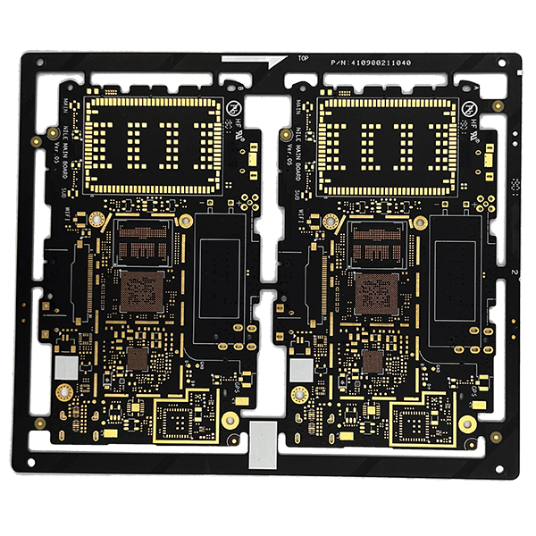
Sophisticated HDI PCB solutions
SEEKPCB's HDI solution includes up to 18 layers any layer hdi of arbitrary interconnect, with a maximum laser hole of 0.3mm and a maximum laser dielectric layer thickness of 0.2mm.
Our HDI technology greatly simplifies the Via on Via process, resulting in faster manufacturing times, higher reliability, and better cost advantages.
HDI PCB Quick Turn Prototype
SEEKPCB has HDI full-process production equipment, and has an independent sample production line, which can quickly respond to HDI samples, small batches, and urgent needs, and we can be competent for the production of HDI rigid-flex boards.
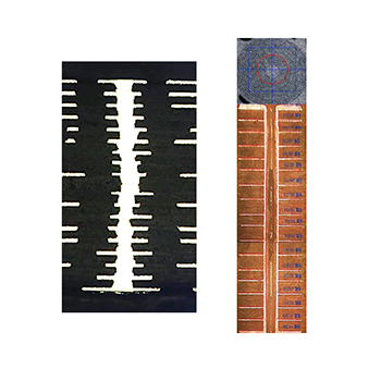
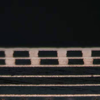
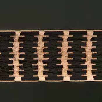
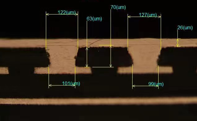
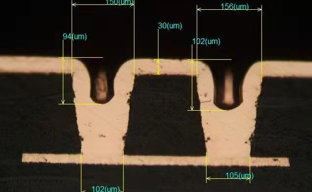
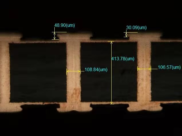
The variety of microvia technologies greatly increases the density of the PCB design and the possibilities for implementation
The Microvias SEEKPCB Can Do
-
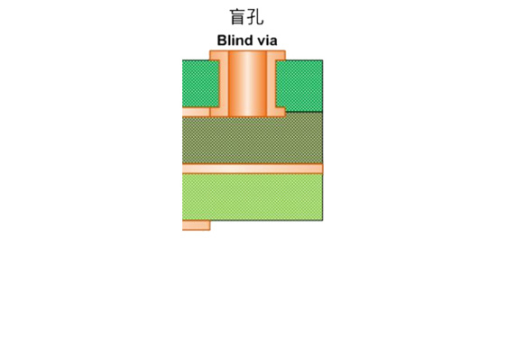
 Blind ViaLearn More
A blind via is a via that connects the outer Layer and inner layer without penetrating the entire board. Blind Via is generally made with laser, but there are also some that are made using mechanical drilling.
-
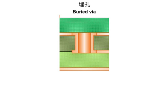
 Buried ViaLearn More
Buried via is made in the inner layer, which is not visible on the top or bottom layer and ais used for signal interconnection in the inner layer.
-
 Mechanical Micro ViaMechanical micro via generally refers to 0.1mm hole machined by mechanical drilling.Learn More


SEEKPCB is well aware of your HDI needs
Why SEEKPCB for your HDI solutions 1
No MOQ
There is no need to worry about high mixed low volume orders, 1pcs orders are just as important for SEEKPCB.
2
Quick Turn HDI
SEEKPCB's quick turn HDI service allows you to get your product to market faster, which is essential for product success.
3
Diverse HDI solutions
SEEKPCB can meet all the processes of HDI, making the design of products easier to implement.
4
Quality first
We are very strict about microvias, in order to make the quality of HDI PCB more reliable and stable.
Our HDI PCB Capability
| Subject | Our Capability |
|---|---|
| Metal Type | FR4(TG150,170, Halogen Free), High Speed, High Frequency, BT |
| Layer | 1-48L |
| Structure | 1)1+N+1 : 1+4+1 thinkness (min)0.35mm 2)2+N+2: 2+4+2 thinkness (min)0.52mm 3)3+N+3: 3+4+3 thinkness (min)0.70mm 4)4+N+4: 4+4+4 thinkness (min)0.87mm |
| Copper Thickness | HOZ - 12OZ |
| Total Thickness | 0.2 - 6.8 mm |
| Insulating layer thickness | 0.03mm |
| Max. board Dimension | 685.8*914.4mm |
| Min Hole Diameter | 0.05mm Laser Via, 0.1mm Mechanical Via |
| Min. line width/spacing | 45um/45um |
| Min BGA Dimension | 0.15mm |
| Special Hole | Blind Hole, Blind Slot, T-Hole, T-Slot, Counter Sink Hole, Cup Hole |
| Surface treatment | OSP, ENIG,Plating Silver, ENEPIG, Immersion Silver, Immersion Tin |
| Outline | Tooling Punching, CNC Routing +/-0.075mm, V-CUT, Laser Routing +/-0.05mm |
SEEKPCB Can Do More For The HDI Solutions
Rigid Flex PCB with HDI Technology
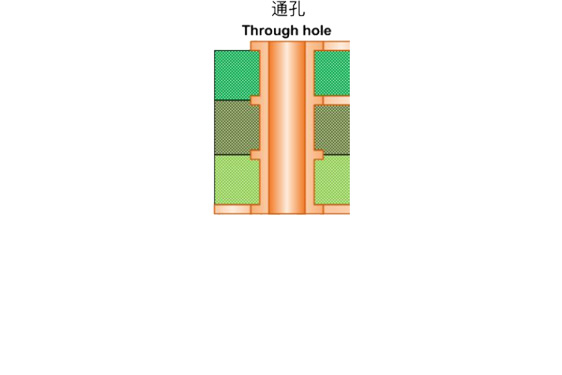
SEEKPCB applies HDI technology to Rigid Flex PCB with Blind Via, Buried Via ,Through Hole, and mixture of them, which provids a better solution for the miniaturization of electronic products. 
What is HDI PCB
HDI (High-Density Interconnect) PCB is a type of printed circuit board that has a higher density of components and interconnections than traditional PCBs. It is designed to provide a more compact, lightweight, and high-performance solution for electronic devices, particularly those that require miniaturization, high speed, and reliability.
HDI PCBs feature microvias, blind vias, and buried vias, which are smaller in diameter and have higher aspect ratios than traditional vias. This allows for a higher density of interconnections and components, reducing the board size and weight, and increasing the signal integrity and speed.
HDI PCBs are used in a wide range of applications, including mobile devices, computer hardware, automotive electronics, medical devices, and more. They offer a number of advantages over traditional PCBs, including improved electrical performance, thermal management, and signal integrity, as well as reduced size, weight, and cost.
The advantages of HDI PCB
HDI PCBs offer several advantages over traditional PCBs, including:
High-density interconnects: HDI PCBs use advanced manufacturing techniques to create high-density interconnects, which means that more components can be placed on a smaller board. This allows for smaller and lighter devices, and also reduces the need for multiple PCBs.
Improved signal performance: HDI PCBs use microvias to provide shorter signal paths and reduce signal loss. This improves signal integrity, reduces noise, and enables faster signal transmission.
Increased reliability: The use of microvias in HDI PCBs also increases the reliability of the board, as it reduces the risk of damage or failure caused by stress, vibration, or thermal expansion.
Better thermal management: HDI PCBs can be designed with thermal vias and metal layers to provide better thermal management, which is important in high-power applications.
Cost-effective: Despite the advanced manufacturing techniques used in HDI PCBs, they can be more cost-effective than traditional PCBs in certain applications. This is because they reduce the need for multiple PCBs and complex assembly processes, and can also be manufactured in larger quantities.
Overall, HDI PCBs offer improved performance, reliability, and cost-effectiveness over traditional PCBs, making them an attractive option for a wide range of electronic applications.
HDI PCB Applications
HDI PCBs are commonly used in a wide range of electronic devices and systems that require high-density interconnects, such as:
Mobile devices: HDI PCBs are widely used in smartphones, tablets, and other mobile devices, where size and weight are critical factors. The use of HDI technology allows for the miniaturization of these devices while also improving their performance and reliability.
Consumer electronics: HDI PCBs are used in various consumer electronic devices, such as digital cameras, gaming consoles, and audio systems. These devices require high-speed interconnects and signal integrity to ensure reliable and high-quality performance.
Medical equipment: HDI PCBs are used in various medical equipment, such as diagnostic imaging devices, patient monitoring systems, and implantable devices. The use of HDI technology in these devices allows for improved performance, reliability, and miniaturization.
Aerospace and defense: HDI PCBs are used in aerospace and defense applications, such as satellites, communication systems, and military equipment. These applications require high reliability, high-frequency interconnects, and thermal management to operate in harsh environments.
Automotive: HDI PCBs are used in various automotive applications, such as advanced driver assistance systems (ADAS), infotainment systems, and engine control units (ECUs). The use of HDI technology in these applications enables better performance, reliability, and miniaturization.
Overall, the use of HDI PCBs is widespread across various industries and applications that require high-density interconnects, improved performance, and miniaturization.
The HDI PCB material
The materials used in HDI PCBs are similar to those used in traditional PCBs, with some variations to accommodate the requirements of high-density interconnects. The materials used in HDI PCBs typically include:
Substrate material: The substrate material is the base layer of the PCB, which provides support for the circuit components and interconnects. The substrate material used in HDI PCBs is usually a high-performance material, such as FR-4, Rogers, or a ceramic-based material, to meet the high-speed and high-frequency requirements of the application.
Conductive materials: The conductive materials used in HDI PCBs include copper, or gold, depending on the application requirements. Copper is the most commonly used material for conductive traces and interconnects, while gold is used for plating and wire bonding.
Dielectric material: The dielectric material is used to insulate the conductive layers and prevent electrical shorts. In HDI PCBs, the dielectric material is typically a high-performance resin, such as epoxy or polyimide, with a lower dielectric constant to reduce signal loss and increase signal integrity.
Vias: HDI PCBs have a higher density of vias, including microvias, blind vias, and buried vias. These vias are made using laser drilling or mechanical drilling techniques and require special materials, such as filled or capped vias, to maintain their integrity and avoid plating issues.
Overall, the materials used in HDI PCBs are selected to meet the specific requirements of the application, including high-speed, high-frequency, and thermal management, while also maintaining the size and weight constraints of the product.
The design rules of HDI PCB?
Designing an HDI PCB requires careful consideration of several design rules to ensure that the board is manufacturable and functions correctly. Some of the key design rules for HDI PCBs include:
Minimum trace and space: HDI PCBs typically require smaller trace and space widths than traditional PCBs, often in the range of 3-4 mils. This requires careful design to ensure that there is no crosstalk or short circuits between adjacent traces.
Minimum via size: HDI PCBs use microvias, which are smaller and more densely packed than traditional vias. The minimum size for microvias varies depending on the manufacturing process used, but is typically around 4-5 mils in diameter.
Staggered vias: Staggered vias are used in HDI PCBs to allow more routing channels within a given area. This requires careful planning to ensure that there is no overlapping or interference between the vias.
Use of blind and buried vias: Blind and buried vias are used in HDI PCBs to reduce the number of layers required and to provide more routing channels. This requires careful planning and design to ensure that the vias do not interfere with other components or traces.
Layer stackup: HDI PCBs often use a complex layer stackup to accommodate the use of microvias, blind and buried vias, and multiple routing layers. The layer stackup must be carefully designed to ensure that there is no interference or crosstalk between the layers.
Overall, designing an HDI PCB requires careful consideration of a range of design rules to ensure that the board is manufacturable and functions correctly.
For more detail please go to our HDI PCB capability.
What are the typical structures of HDI pcb?
There are several typical structures used in HDI PCB design, including:
1+N+1: This structure consists of a single layer on one side of the board, followed by a number of layers with buried vias, and then a single layer on the other side of the board. This structure is commonly used in smartphones and other mobile devices.
2+N+2: This structure consists of two outer layers with blind vias, followed by a number of layers with buried vias, and then another two outer layers with blind vias. This structure is commonly used in high-density servers, high-speed networking equipment, and other applications that require high performance.
Any-layer interstitial via hole (AIIVH): This structure consists of microvias that are drilled through all layers of the board, allowing for maximum routing density and improved signal integrity. This structure is commonly used in high-performance computing and other applications that require high speed and high reliability.
Build-up HDI: This structure uses multiple layers of thin dielectric material with conductive features to build up the circuitry, allowing for maximum routing density and flexibility. This structure is commonly used in wearable devices, medical devices, and other applications where space and weight are at a premium.
Overall, the choice of HDI PCB structure will depend on the specific requirements of the application, including size, weight, performance, and cost.
What are the difficulties in IC substrate manufacturing?
There are several challenges and difficulties in HDI PCB manufacture, including:
Increased complexity: HDI PCBs have much higher complexity than traditional PCBs, with much finer line and space requirements, more layers, and smaller vias. This complexity can make it difficult to design and manufacture the boards, and can also increase the risk of defects and failures.
High precision manufacturing: HDI PCBs require much higher precision in manufacturing, with tighter tolerances for drilling, plating, and other processes. This precision can be difficult to achieve, and requires advanced equipment and skilled operators.
High aspect ratio drilling: HDI PCBs often require very small and deep holes, known as microvias, which can have very high aspect ratios (the ratio of the depth to the diameter of the hole). These high aspect ratio holes can be difficult to drill and plate, and can also increase the risk of defects and failures.
Material selection: HDI PCBs often require specialized materials, such as thin copper foils, high-Tg (glass transition temperature) laminates, and low-loss dielectrics, to meet the requirements for high density and high speed. These materials can be more expensive and difficult to source than standard PCB materials.
Overall, the manufacturing of HDI PCBs requires advanced equipment, skilled operators, and careful attention to detail throughout the process. It is important to work with an experienced PCB manufacturer who has the expertise and resources to produce high-quality HDI PCBs.
How to optimize HDI PCB design for better cost and reliability
Optimizing the design of an HDI PCB can help improve its cost and reliability. Here are some tips to consider:
Reduce the number of layers: One way to reduce the cost of an HDI PCB is to reduce the number of layers. This can be achieved by using blind and buried vias, which allow for more routing on fewer layers. However, reducing the number of layers may also reduce the performance and functionality of the PCB.
Use standard materials: Using standard materials wherever possible can help reduce the cost of an HDI PCB. However, it is important to choose materials that still meet the performance requirements of the PCB.
Optimize the via design: The via design is critical to the performance and reliability of an HDI PCB. Using microvias can help reduce the size of the board and increase routing density, but it can also increase the cost of the PCB. Therefore, it is important to optimize the via design to balance performance and cost.
Minimize the use of blind and buried vias: While blind and buried vias can help reduce the number of layers and increase routing density, they are also more difficult and expensive to manufacture. Minimizing their use can help reduce the cost and complexity of the PCB.
Consider design for manufacturability: Designing the PCB with manufacturability in mind can help reduce the cost and increase the reliability of the PCB. For example, avoiding complex geometries and using standard drill sizes can help reduce the cost and improve the yield of the PCB.
Work closely with the manufacturer: Working closely with the manufacturer can help ensure that the design is optimized for cost and reliability. The manufacturer can provide valuable insights into the manufacturability of the design, and can suggest ways to optimize the design for cost and reliability.
How to ensure the quality in HDI PCB manufacturing?
There are several steps that can be taken to ensure quality in HDI PCB manufacturing:
Design for Manufacturability (DFM): The first step in ensuring quality is to ensure that the design of the HDI PCB is manufacturable. This involves designing the PCB in such a way that it can be fabricated with minimal errors and defects.
Material Selection: The choice of materials used in the manufacturing of HDI PCBs can have a significant impact on the final product's quality. The materials used should be of high quality and chosen with the specific application and requirements of the PCB in mind.
Quality Control during Manufacturing: Quality control measures should be put in place during every step of the manufacturing process, including the application of solder paste, component placement, soldering, and testing.
Testing and Inspection: HDI PCBs should be tested and inspected at various stages of the manufacturing process to identify and correct any defects or issues. This includes automated optical inspection (AOI) and X-ray inspection to ensure the accuracy of component placement and solder joints.
Continuous Improvement: To ensure that quality is maintained, the manufacturing process should be continuously reviewed and improved upon. This involves identifying areas for improvement and implementing changes to address any issues and ensure consistent quality.
Overall, ensuring quality in HDI PCB manufacturing requires a commitment to excellence at every step of the process, from design to testing and continuous improvement.
+86-20-82192100
+86-18925293263
+86-18925293263
B206, Xihuan Road, Shajing, Baoan district, Shenzhen
About SEEKPCB
SEEKPCB is specializing in electronics one stop solution, including PCB design, PCB manufacturing, PCB Assembly, Component sourcing. Quick turn PCB prototype, express PCB assembly are our strengths to fullfil fast time-to-market and your vitory.
Quick Links
Subsribe Now
Sign up for our newsletter to receive the latest news.


